ICIECA 2014 Paper 07
Download as PPTX, PDF•1 like•424 views

A novel voltage-mode look-up table using a clock boosting technique in standard CMOS has been designed. The proposed quaternary logic implementation reduces power and delay by overcoming drawbacks of previous techniques. It uses a standard CMOS technology and clock boosting technique to enhance speed without increasing power consumption. The quaternary look-up table reduces the number of gates in the decoder and multiplexer, resulting in lower power compared to existing binary implementations.
![REFRENCES
[1] J. Rabaey, Low Power Design Essentials (Integrated Circuits and
Systems). New York, NY, USA: Springer-Verlag, 2009.
[2] L. Shang, A. S. Kaviani, and K. Bathala, “Dynamic power
consumption
in virtex-II FPGA family,” in Proc. ACM/SIGDA Int. Symp. Field-
Program. Gate Arrays, 2002, pp. 157–164.
[3] Z. Zilic and Z. Vranesic, “Multiple-valued logic in FPGAs,” in
Proc.
Midwest Symp. Circuits Syst., 1993, pp. 1553–1556.
[4] E. Ozer, R. Sendag, and D. Gregg, “Multiple-valued logic buses for
reducing bus energy in low-power systems,” IEE Comput. Digital
Tech.,vol. 153, no. 4, pp. 270–282, Jul. 2006.
[5] K. Current, “Current-mode CMOS multiple-valued logic circuits,”
IEEE J. Solid-State Circuits, vol. 29, no. 2, pp. 95–107, Feb. 1994.](https://image.slidesharecdn.com/07-141220015252-conversion-gate02/85/ICIECA-2014-Paper-07-28-320.jpg)

ICIECA 2014 Paper 07
- 1. A NOVEL VOLTAGE-MODE LUT USING CLOCK BOOSTING TECHNIQUE IN STANDARD CMOS BY SATHYAVATHI N S ME-VLSI DESIGN
- 2. CONTENT • INTRODUCTION • OBJECTIVE • EXISTING SYSTEM • PROBLEM FORMULATION • PROPOSED SYSTEM • TOOLS REQUIRED • OUTPUT • SUMMARY • REFERENCES
- 3. INTRODUCTION The Interconnections plays the dominant role in VLSI system On reducing the interconnection we can able to reduce Delay, Power, Area. So now many techniques has been found to reduce the interconnections
- 4. OBJECTIVE • Reducing the routing leads to a direct reduction of the line capacitances and the overall circuit area. • Thus the Quaternary logic helps to implement more logic function then the binary logic
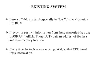
- 5. EXISTING SYSTEM Look up Table are used especially in Non Volatile Memories like ROM In order to get their information from these memories they use LOOK UP TABLE. These LUT contains address of the data and their memory location. Every time the table needs to be updated, so that CPU could fetch information.
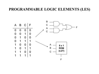
- 6. PROGRAMMABLE LOGIC ELEMENTS (LES) A B C F 0 0 0 0 0 0 1 0 0 1 0 0 0 1 1 1 1 0 0 0 1 0 1 1 1 1 0 0 1 1 1 1 B C A C F 8 x 1 ROM (LUT) A B C F
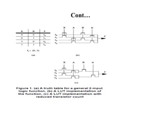
- 7. Cont…
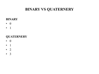
- 8. BINARY VS QUATERNERY BINARY • 0 • 1 QUATERNERY • 0 • 1 • 2 • 3
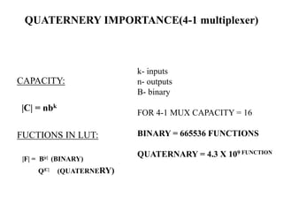
- 9. QUATERNERY IMPORTANCE(4-1 multiplexer) CAPACITY: |C| = nbk FUCTIONS IN LUT: |F| = B|c| (BINARY) Q|C| (QUATERNERY) k- inputs n- outputs B- binary FOR 4-1 MUX CAPACITY = 16 BINARY = 665536 FUNCTIONS QUATERNARY = 4.3 X 10⁹ FUNCTION
- 10. PROBLEM FORMULATION Clock boosting techniques cannot be implemented. Slower speed More interconnection has to be found. Complexity is more
- 11. PROPOSED • Using the quaternary look up table more functions has to be implemented. • Reducing the routing leads to a direct reduction of the line capacitances and the overall circuit area. • Consume less power • Transistor count has been reduced • Implementation of clock boosting techniques.
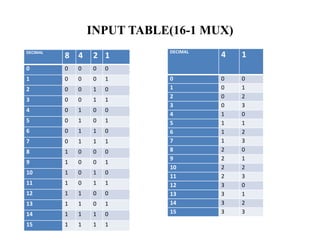
- 12. INPUT TABLE(16-1 MUX) DECIMAL 8 4 2 1 0 0 0 0 0 1 0 0 0 1 2 0 0 1 0 3 0 0 1 1 4 0 1 0 0 5 0 1 0 1 6 0 1 1 0 7 0 1 1 1 8 1 0 0 0 9 1 0 0 1 10 1 0 1 0 11 1 0 1 1 12 1 1 0 0 13 1 1 0 1 14 1 1 1 0 15 1 1 1 1 DECIMAL 4 1 0 0 0 1 0 1 2 0 2 3 0 3 4 1 0 5 1 1 6 1 2 7 1 3 8 2 0 9 2 1 10 2 2 11 2 3 12 3 0 13 3 1 14 3 2 15 3 3
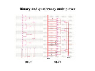
- 13. Binary and quaternary multiplexer BLUT QLUT
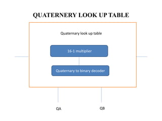
- 14. QUATERNERY LOOK UP TABLE 16-1 multiplier Quaternary to binary decoder Quaternary look up table QA QB
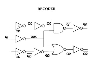
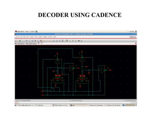
- 15. DECODER
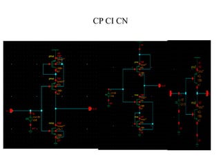
- 16. CP CI CN
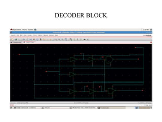
- 17. DECODER BLOCK
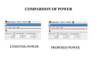
- 20. COMPARISON OF POWER EXSISTING POWER PROPOSED POWER
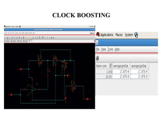
- 21. CLOCK BOOSTING
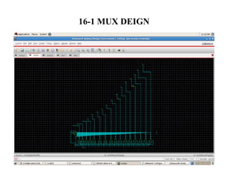
- 22. 16-1 MUX DEIGN
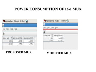
- 23. POWER CONSUMPTION OF 16-1 MUX PROPOSED MUX MODIFIED MUX
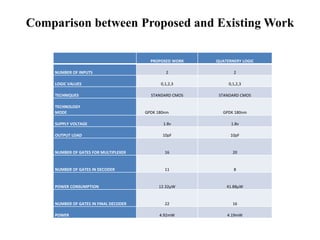
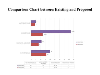
- 24. Comparison between Proposed and Existing Work PROPOSED WORK QUATERNERY LOGIC NUMBER OF INPUTS 2 2 LOGIC VALUES 0,1,2,3 0,1,2,3 TECHNIQUES STANDARD CMOS STANDARD CMOS TECHNOLOGY MODE GPDK 180nm GPDK 180nm SUPPLY VOLTAGE 1.8v 1.8v OUTPUT LOAD 10pF 10pF NUMBER OF GATES FOR MULTIPLEXER 16 20 NUMBER OF GATES IN DECODER 11 8 POWER CONSUMPTION 12.32µW 41.88µW NUMBER OF GATES IN FINAL DECODER 22 16 POWER 4.92mW 4.19mW
- 25. Comparison Chart between Existing and Proposed 16 8 12.32 4 20 11 41.88 5 0 5 10 15 20 25 30 35 40 45 NO.OF GATES(MUX) NO OF GATES IN DECODER DECODER POWER MULTIPLEXER POWER NO.OF GATES(MUX) NO OF GATES IN DECODER DECODER POWER MULTIPLEXER POWER EXSISTING 20 11 41.88 5 PROPOSED 16 8 12.32 4 EXSISTING PROPOSED
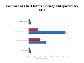
- 26. Comparison Chart between Binary and Quaternary LUT 4 30 64 4 2 20 16 2 0 10 20 30 40 50 60 70 No.of Inputs No.of transmission gates No.of functions in LUT 2-1 MUX DECIMAL TO LOGIC QUATERNERY BINARY
- 27. SUMMARY A new look-up table structure based on a low-power high-speed quaternary voltage-mode device had been designed. Our quaternary implementation overcomes the drawbacks of previously proposed techniques by using a standard CMOS technology reduces the power and delay.. A clock boosting technique to enhance speed without increasing consumption.
- 28. REFRENCES [1] J. Rabaey, Low Power Design Essentials (Integrated Circuits and Systems). New York, NY, USA: Springer-Verlag, 2009. [2] L. Shang, A. S. Kaviani, and K. Bathala, “Dynamic power consumption in virtex-II FPGA family,” in Proc. ACM/SIGDA Int. Symp. Field- Program. Gate Arrays, 2002, pp. 157–164. [3] Z. Zilic and Z. Vranesic, “Multiple-valued logic in FPGAs,” in Proc. Midwest Symp. Circuits Syst., 1993, pp. 1553–1556. [4] E. Ozer, R. Sendag, and D. Gregg, “Multiple-valued logic buses for reducing bus energy in low-power systems,” IEE Comput. Digital Tech.,vol. 153, no. 4, pp. 270–282, Jul. 2006. [5] K. Current, “Current-mode CMOS multiple-valued logic circuits,” IEEE J. Solid-State Circuits, vol. 29, no. 2, pp. 95–107, Feb. 1994.