

2q
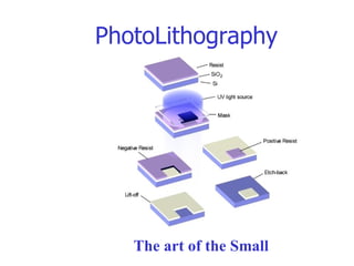
- 1. PhotoLithography The art of the Small
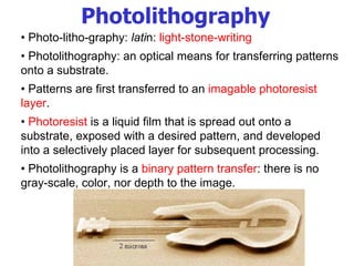
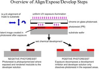
- 11. • Photo-litho-graphy: lati n: light-stone-writing • Photolithography: an optical means for transferring patterns onto a substrate. • Patterns are first transferred to an imagable photoresist layer . • Photoresist is a liquid film that is spread out onto a substrate, exposed with a desired pattern, and developed into a selectively placed layer for subsequent processing. • Photolithography is a binary pattern transfer : there is no gray-scale, color, nor depth to the image. Photolithography
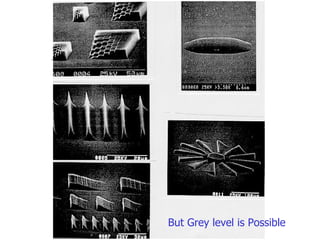
- 12. But Grey level is Possible
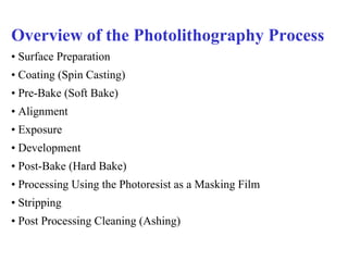
- 17. Overview of the Photolithography Process • Surface Preparation • Coating (Spin Casting) • Pre-Bake (Soft Bake) • Alignment • Exposure • Development • Post-Bake (Hard Bake) • Processing Using the Photoresist as a Masking Film • Stripping • Post Processing Cleaning (Ashing)
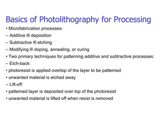
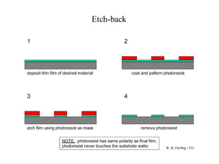
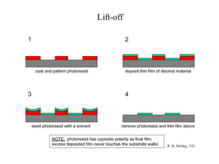
- 20. Basics of Photolithography for Processing • Microfabrication processes: – Additive ® deposition – Subtractive ® etching – Modifying ® doping, annealing, or curing • Two primary techniques for patterning additive and subtractive processes: – Etch-back: • photoresist is applied overtop of the layer to be patterned • unwanted material is etched away – Lift-off: • patterned layer is deposited over top of the photoresist • unwanted material is lifted off when resist is removed
- 23. Wafer Cleaning • Typical contaminants that must be removed prior to photoresist coating: • dust from scribing or cleaving (minimized by laser scribing) • atmospheric dust (minimized by good clean room practice) • abrasive particles (from lapping or CMP) • lint from wipers (minimized by using lint-free wipers) • photoresist residue from previous photolithography (minimized by performing oxygen plasma ashing) • bacteria (minimized by good DI water system) • films from other sources: – solvent residue – H 2 O residue – photoresist or developer residue – oil – silicone
- 24. Wafer Priming • Adhesion promoters are used to assist resist coating. • Resist adhesion factors: • moisture content on surface • wetting characteristics of resist • type of primer • delay in exposure and prebake • resist chemistry • surface smoothness • stress from coating process • surface contamination • Ideally want no H 2 O on wafer surface – Wafers are given a “singe” step prior to priming and coating 15 minutes in 80-90°C convection oven
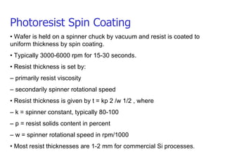
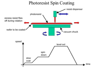
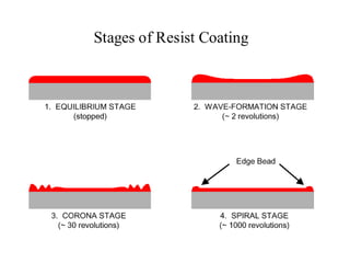
- 25. Photoresist Spin Coating • Wafer is held on a spinner chuck by vacuum and resist is coated to uniform thickness by spin coating. • Typically 3000-6000 rpm for 15-30 seconds. • Resist thickness is set by: – primarily resist viscosity – secondarily spinner rotational speed • Resist thickness is given by t = kp 2 /w 1/2 , where – k = spinner constant, typically 80-100 – p = resist solids content in percent – w = spinner rotational speed in rpm/1000 • Most resist thicknesses are 1-2 mm for commercial Si processes .
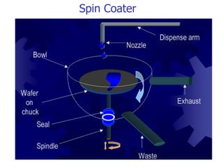
- 26. Spin Coater
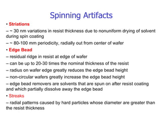
- 30. Spinning Artifacts • Striations – ~ 30 nm variations in resist thickness due to nonuniform drying of solvent during spin coating – ~ 80-100 mm periodicity, radially out from center of wafer • Edge Bead – residual ridge in resist at edge of wafer – can be up to 20-30 times the nominal thickness of the resist – radius on wafer edge greatly reduces the edge bead height – non-circular wafers greatly increase the edge bead height – edge bead removers are solvents that are spun on after resist coating and which partially dissolve away the edge bead • Streaks – radial patterns caused by hard particles whose diameter are greater than the resist thickness
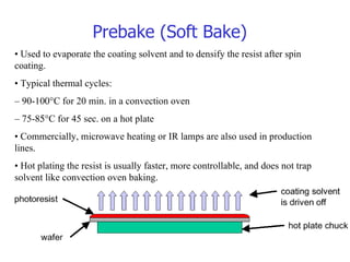
- 31. Prebake (Soft Bake) • Used to evaporate the coating solvent and to densify the resist after spin coating. • Typical thermal cycles: – 90-10 °C for 20 min. in a convection oven – 75-8 °C for 45 sec. on a hot plate • Commercially, microwave heating or IR lamps are also used in production lines. • Hot plating the resist is usually faster, more controllable, and does not trap solvent like convection oven baking.
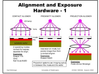
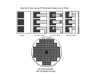
- 34. Alignment and Exposure Hardware - 2 – For simple contact, proximity, and projection systems, the mask is the same size and scale as the printed wafer pattern. I.e. the reproduction ratio is 1:1. – Projection systems give the ability to change the reproduction ratio. Going to 10:1 reduction allows larger size patterns on the mask, which is more robust to mask defects. – Mask size can get unwieldy for large wafers. – Most wafers contain an array of the same pattern, so only one cell of the array is needed on the mask. This system is called Direct Step on Wafer (DSW). These machines are also called “Steppers” – Advantage of steppers: only 1 cell of wafer is needed – Disadvantage of steppers: the 1 cell of the wafer on the mask must be perfect-- absolutely no defects, since it gets used for all die.
- 35. Alignment and Exposure Hardware - 3 – Higher end research systems go one step further and use Direct Write on Wafer (DWW) exposure systems. – This can be accomplished using: • Excimer lasers for geometries down to 1-2 mm • Electron beams for geometries down to 0.1-0.2 mm • Focused ion beams for geometries down to 0.05-0.1 mm – No mask is needed for these technologies. – These are serial processes, and wafer cycle time is proportional to the beam writing time-- the smaller the spot, the longer it takes!
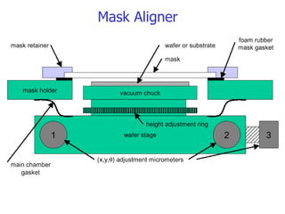
- 36. Mask Aligner
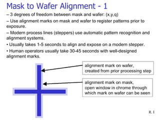
- 37. Mask to Wafer Alignment - 1 – 3 degrees of freedom between mask and wafer: (x,y,q) – Use alignment marks on mask and wafer to register patterns prior to exposure. – Modern process lines (steppers) use automatic pattern recognition and alignment systems. • Usually takes 1-5 seconds to align and expose on a modern stepper. • Human operators usually take 30-45 seconds with well-designed alignment marks.
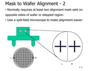
- 38. Mask to Wafer Alignment - 2 • Normally requires at least two alignment mark sets on opposite sides of wafer or stepped region. • Use a split-field microscope to make alignment easier:
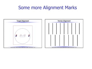
- 39. Some more Alignment Marks
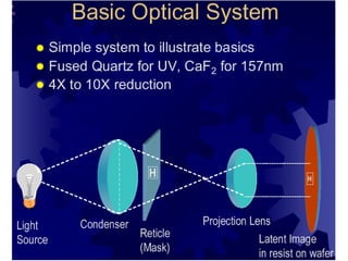
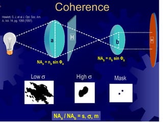
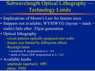
- 40. Optical Exposure Projection Optics Numerical Aperture Raleigh Criterion Coherence Optical Correction & Phase Shift Selection
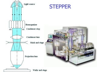
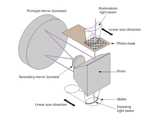
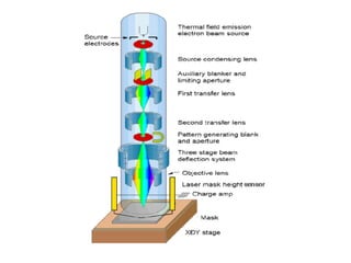
- 44. STEPPER
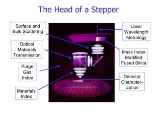
- 45. The Head of a Stepper
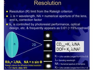
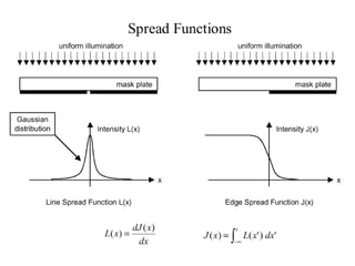
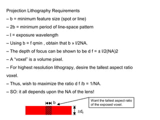
- 51. Projection Lithography Requirements – b = minimum feature size (spot or line) – 2b = minimum period of line-space pattern – l = exposure wavelength – Using b = f qmin , obtain that b » l/2NA. – The depth of focus can be shown to be d f = ± l/2(NA)2 – A “voxel” is a volume pixel. – For highest resolution lithograpy, desire the tallest aspect ratio voxel. – Thus, wish to maximize the ratio d f /b = 1/NA. – SO: it all depends upon the NA of the lens!
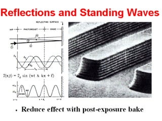
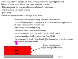
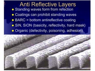
- 54. • Short exposure wavelengths can create standing waves in a layer of photoresist. Regions of constructive interference create increased exposure. • These can impair the structure of the resist, but can be eliminated by: – use of multiple wavelength sources – postbaking • Effects are most noticeable at the edge of the resist. • Standing waves are enhanced by reflective wafer surfaces. • If the wafer or substrate is transparent, reflections from the aligner chuck can create standing wave patterns, also. – This can be eliminated by using: • a flat black chuck (anodized aluminum) • an optical absorber under the wafer (lint free black paper) • a transparent glass chuck (used on Karl Suss MJB3) • Exposures can be greatly miscalculated by the presence of standing waves and reflective wafers or chucks.
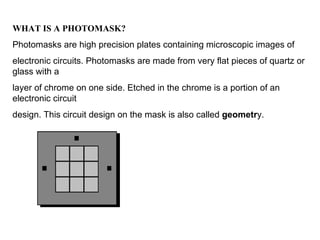
- 59. WHAT IS A PHOTOMASK? Photomasks are high precision plates containing microscopic images of electronic circuits. Photomasks are made from very flat pieces of quartz or glass with a layer of chrome on one side. Etched in the chrome is a portion of an electronic circuit design. This circuit design on the mask is also called geometr y.
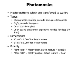
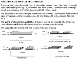
- 61. MATERIAL USED TO MAKE PHOTOMASKS: There are four types of material used to make photomasks; quartz (the most commonly used and most expensive), LE, soda lime, and white crown. The mask sizes can range from 3 inches square to 7 inches square and 7.25 inches round. The thickness of the masks ranges from 60 mils to 250 mils. Currently the most common sizes of masks used are 5 inches square 90 mils thick and 6 inches square 250 mils thick. The quartz or glass (or substrat e) has a layer of chrome on one side. The chrome is covered with an AR (anti-reflective) coating and a photosensitive resis t. The substrate with chrome, AR, and resist is known as a blank.
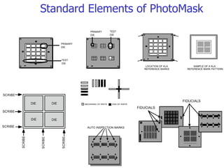
- 62. Standard Elements of PhotoMask
- 66. Postbake (Hard Bake) - 1 • Used to stabilize and harden the developed photoresist prior to processing steps that the resist will mask. • Main parameter is the plastic flow or glass transition temperature. • Postbake removes any remaining traces of the coating solvent or developer. • This eliminates the solvent burst effects in vacuum processing. • Postbake introduces some stress into the photoresist. • Some shrinkage of the photoresist may occur. • Longer or hotter postbake makes resist removal much more difficult.
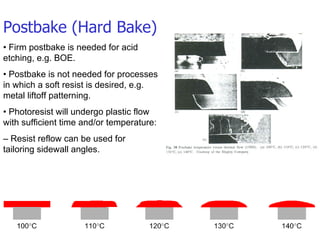
- 67. Postbake (Hard Bake) • Firm postbake is needed for acid etching, e.g. BOE. • Postbake is not needed for processes in which a soft resist is desired, e.g. metal liftoff patterning. • Photoresist will undergo plastic flow with sufficient time and/or temperature: – Resist reflow can be used for tailoring sidewall angles.
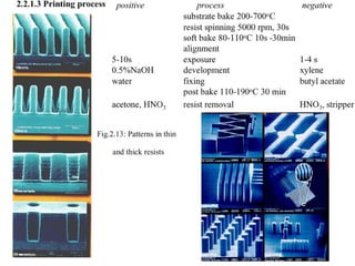
- 68. Photoresist Removal (Stripping) • Want to remove the photoresist and any of its residues. • Simple solvents are generally sufficient for non-postbaked photoresists: – Positive photoresists: • acetone • trichloroethylene (TCE) • phenol-based strippers (Indus-Ri-Chem J-100) – Negative photoresists: • methyl ethyl ketone (MEK), CH 3 COC 2 H 5 • methyl isobutyl ketone (MIBK), CH 3 COC 4 H 9 • Plasma etching with O 2 (ashing) is also effective for removing organic polymer debris. – Also: Shipley 1165 stripper (contains n-methyl-2-pyrrolidone), which is effective on hard, postbaked resist.
- 69. PhotoResist
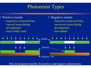
- 75. Advantages of Positive Photoresists • Most commonly used in the IC industry. • Superior to negative photoresists because: – They do not swell during development. – They are capable of finer resolution. – They are reasonably resistant to plasma processing operations. Positive PhotoResist
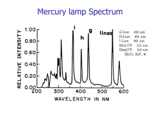
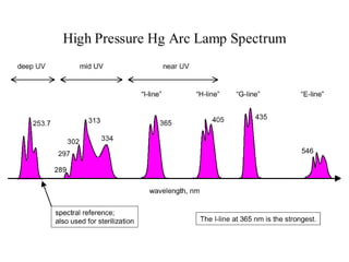
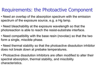
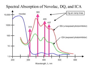
- 77. Requirements: the Photoactive Component • Need an overlap of the absorption spectrum with the emission spectrum of the exposure source, e.g. a Hg lamp. • Need bleachability at the exposure wavelength so that the photoreaction is able to reach the resist-substrate interface. • Need compatibility with the base resin (novolac) so that the two form a single, miscible phase. • Need thermal stability so that the photoactive dissolution inhibitor does not break down at prebake temperatures. • Photoactive dissolution inhibitors are often modified to alter their spectral absorption, thermal stability, and miscibility characteristics.
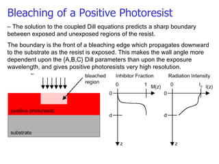
- 78. Bleaching of a Positive Photoresist – The solution to the coupled Dill equations predicts a sharp boundary between exposed and unexposed regions of the resist. The boundary is the front of a bleaching edge which propagates downward to the substrate as the resist is exposed. This makes the wall angle more dependent upon the {A,B,C} Dill parameters than upon the exposure wavelength, and gives positive photoresists very high resolution.
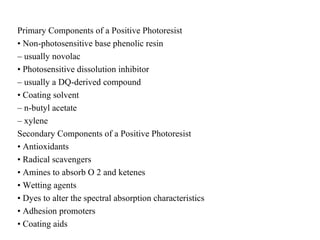
- 80. Primary Components of a Positive Photoresist • Non-photosensitive base phenolic resin – usually novolac • Photosensitive dissolution inhibitor – usually a DQ-derived compound • Coating solvent – n-butyl acetate – xylene Secondary Components of a Positive Photoresist • Antioxidants • Radical scavengers • Amines to absorb O 2 and ketenes • Wetting agents • Dyes to alter the spectral absorption characteristics • Adhesion promoters • Coating aids
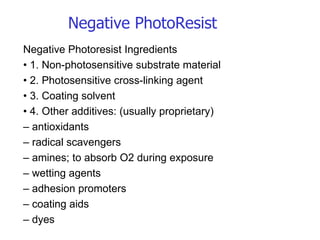
- 82. Negative Photoresist Ingredients • 1. Non-photosensitive substrate material • 2. Photosensitive cross-linking agent • 3. Coating solvent • 4. Other additives: (usually proprietary) – antioxidants – radical scavengers – amines; to absorb O2 during exposure – wetting agents – adhesion promoters – coating aids – dyes Negative PhotoResist
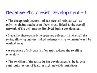
- 83. Negative Photoresist Development - 1 • The unexposed (uncross-linked) areas of resist as well as polymer chains that have not been cross-linked to the overall network of the gel must be dissolved during development. • Negative photoresist developers are solvents which swell the resist, allowing uncross-linked polymer chains to untangle and be washed away. • A sequence of solvents is often used to keep the swelling reversible. • The swelling of the resist during development is the largest contributor to loss of features and linewidth limitations.
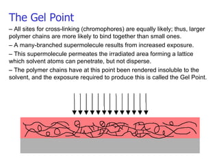
- 84. The Gel Point – All sites for cross-linking (chromophores) are equally likely; thus, larger polymer chains are more likely to bind together than small ones. – A many-branched supermolecule results from increased exposure. – This supermolecule permeates the irradiated area forming a lattice which solvent atoms can penetrate, but not disperse. – The polymer chains have at this point been rendered insoluble to the solvent, and the exposure required to produce this is called the Gel Point.